Product Datasheet Search Results:
 1 Pages, 100 KB, Original
- 2N696
- Advanced Semiconductor, Inc.
- 40 V, NPN, Si, SMALL SIGNAL TRANSISTOR, TO-5
 5 Pages, 116 KB, Scan
- 2N696
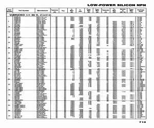
- Thomson-csf
- Signal Transistors and Field Effect Transistors 1976
 1 Pages, 98 KB, Scan
- 2N696
- Continental Device India Limited
- Semiconductor Device Data Book 1996
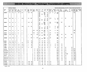
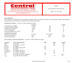
 1 Pages, 461 KB, Original
- 2N696
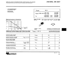
- Central Semiconductor Corp.
- 40 V, NPN, Si, SMALL SIGNAL TRANSISTOR, TO-39
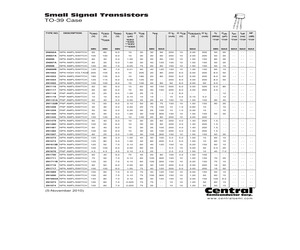
 2 Pages, 105 KB, Original
- 2N696LEADFREE
- Central Semiconductor Corp.
- 40 V, NPN, Si, SMALL SIGNAL TRANSISTOR, TO-39
 1 Pages, 80 KB, Scan
- 2N696
- Ferranti Semiconductors
- Shortform Data Book 1971
Product Details Search Results:
Advancedsemiconductor.com/2N696
{"Status":"ACTIVE","Package Body Material":"METAL","Mfr Package Description":"TO-5, 3 PIN","Terminal Form":"WIRE","Package Style":"CYLINDRICAL","DC Current Gain-Min (hFE)":"40","Collector-emitter Voltage-Max":"40 V","Transistor Element Material":"SILICON","Transition Frequency-Nom (fT)":"80 MHz","Terminal Position":"BOTTOM","Transistor Polarity":"NPN","Package Shape":"ROUND","Configuration":"SINGLE","Transistor Type":"GENERAL PURPOSE SMALL SIGNAL","Number of Terminals":"3","Number of Elements":"1"}...
1198 Bytes - 02:21:22, 19 October 2024
Centralsemi.com/2N696
{"Status":"ACTIVE","Terminal Finish":"TIN LEAD","Package Body Material":"METAL","Mfr Package Description":"TO-39, 3 PIN","Terminal Form":"WIRE","Package Style":"CYLINDRICAL","DC Current Gain-Min (hFE)":"20","Collector-emitter Voltage-Max":"40 V","Transistor Application":"SWITCHING","Transition Frequency-Nom (fT)":"80 MHz","Transistor Element Material":"SILICON","Terminal Position":"BOTTOM","Transistor Polarity":"NPN","Package Shape":"ROUND","Configuration":"SINGLE","Transistor Type":"GENERAL PURPOSE SMALL S...
1252 Bytes - 02:21:22, 19 October 2024
Centralsemi.com/2N696LEADFREE
{"Status":"ACTIVE","Lead Free":"Yes","Terminal Finish":"MATTE TIN (315)","Package Body Material":"METAL","Mfr Package Description":"TO-39, 3 PIN","Terminal Form":"WIRE","Package Style":"CYLINDRICAL","DC Current Gain-Min (hFE)":"20","Collector-emitter Voltage-Max":"40 V","Transistor Application":"SWITCHING","Transition Frequency-Nom (fT)":"80 MHz","Transistor Element Material":"SILICON","EU RoHS Compliant":"Yes","Terminal Position":"BOTTOM","Transistor Polarity":"NPN","Package Shape":"ROUND","Configuration":...
1354 Bytes - 02:21:22, 19 October 2024
Dla.mil/2N6966+JANTX
{"C(iss) Max. (F)":"1.8p","Absolute Max. Power Diss. (W)":"70","r(DS)on Max. (Ohms)":"85m","@V(DS) (V) (Test Condition)":"15","I(GSS) Max. (A)":"100n","V(BR)GSS (V)":"30","@I(D) (A) (Test Condition)":"3.0","@(VDS) (V) (Test Condition)":"30","Package":"TO-213AA","I(DSS) Min. (A)":"250u","Military":"Y","Mil Number":"JANTX2N6966","t(r) Max. (s) Rise time":"60n","V(BR)DSS (V)":"100","t(f) Max. (s) Fall time.":"30n","g(fs) Min. (S) Trans. conduct.":"6.0","I(D) Abs. Drain Current (A)":"20"}...
1020 Bytes - 02:21:22, 19 October 2024
Dla.mil/2N6966+JANTXV
{"C(iss) Max. (F)":"1.8p","Absolute Max. Power Diss. (W)":"70","r(DS)on Max. (Ohms)":"85m","@V(DS) (V) (Test Condition)":"15","I(GSS) Max. (A)":"100n","V(BR)GSS (V)":"30","@I(D) (A) (Test Condition)":"3.0","@(VDS) (V) (Test Condition)":"30","Package":"TO-213AA","I(DSS) Min. (A)":"250u","Military":"Y","Mil Number":"JANTXV2N6966","t(r) Max. (s) Rise time":"60n","V(BR)DSS (V)":"100","t(f) Max. (s) Fall time.":"30n","g(fs) Min. (S) Trans. conduct.":"6.0","I(D) Abs. Drain Current (A)":"20"}...
1026 Bytes - 02:21:22, 19 October 2024
Dla.mil/2N6967+JANTX
{"C(iss) Max. (F)":"1.8p","Absolute Max. Power Diss. (W)":"70","r(DS)on Max. (Ohms)":"180m","@V(DS) (V) (Test Condition)":"15","I(GSS) Max. (A)":"100n","V(BR)GSS (V)":"30","@I(D) (A) (Test Condition)":"3.0","@(VDS) (V) (Test Condition)":"30","Package":"TO-213AA","I(DSS) Min. (A)":"250u","Military":"Y","Mil Number":"JANTX2N6967","t(r) Max. (s) Rise time":"60n","V(BR)DSS (V)":"200","t(f) Max. (s) Fall time.":"60n","g(fs) Min. (S) Trans. conduct.":"6.0","I(D) Abs. Drain Current (A)":"13"}...
1021 Bytes - 02:21:22, 19 October 2024
Dla.mil/2N6967+JANTXV
{"C(iss) Max. (F)":"1.8p","Absolute Max. Power Diss. (W)":"70","r(DS)on Max. (Ohms)":"180m","@V(DS) (V) (Test Condition)":"15","I(GSS) Max. (A)":"100n","V(BR)GSS (V)":"30","@I(D) (A) (Test Condition)":"3.0","@(VDS) (V) (Test Condition)":"30","Package":"TO-213AA","I(DSS) Min. (A)":"250u","Military":"Y","Mil Number":"JANTXV2N6967","t(r) Max. (s) Rise time":"60n","V(BR)DSS (V)":"200","t(f) Max. (s) Fall time.":"60n","g(fs) Min. (S) Trans. conduct.":"6.0","I(D) Abs. Drain Current (A)":"13"}...
1027 Bytes - 02:21:22, 19 October 2024
Dla.mil/2N6968+JANTX
{"C(iss) Max. (F)":"1.6p","Absolute Max. Power Diss. (W)":"70","r(DS)on Max. (Ohms)":"550m","@V(DS) (V) (Test Condition)":"15","I(GSS) Max. (A)":"100n","V(BR)GSS (V)":"30","@I(D) (A) (Test Condition)":"2.0","@(VDS) (V) (Test Condition)":"30","Package":"TO-213AA","I(DSS) Min. (A)":"250u","Military":"Y","Mil Number":"JANTX2N6968","t(r) Max. (s) Rise time":"15n","V(BR)DSS (V)":"400","t(f) Max. (s) Fall time.":"35n","g(fs) Min. (S) Trans. conduct.":"4.0","I(D) Abs. Drain Current (A)":"7.5"}...
1022 Bytes - 02:21:22, 19 October 2024
Dla.mil/2N6968+JANTXV
{"C(iss) Max. (F)":"1.6p","Absolute Max. Power Diss. (W)":"70","r(DS)on Max. (Ohms)":"550m","@V(DS) (V) (Test Condition)":"15","I(GSS) Max. (A)":"100n","V(BR)GSS (V)":"30","@I(D) (A) (Test Condition)":"2.0","@(VDS) (V) (Test Condition)":"30","Package":"TO-213AA","I(DSS) Min. (A)":"250u","Military":"Y","Mil Number":"JANTXV2N6968","t(r) Max. (s) Rise time":"15n","V(BR)DSS (V)":"400","t(f) Max. (s) Fall time.":"35n","g(fs) Min. (S) Trans. conduct.":"4.0","I(D) Abs. Drain Current (A)":"7.5"}...
1028 Bytes - 02:21:22, 19 October 2024
Dla.mil/2N6969+JANTX
{"C(iss) Max. (F)":"1.6p","Absolute Max. Power Diss. (W)":"70","r(DS)on Max. (Ohms)":"850m","@V(DS) (V) (Test Condition)":"15","I(GSS) Max. (A)":"100n","V(BR)GSS (V)":"30","@I(D) (A) (Test Condition)":"2.0","@(VDS) (V) (Test Condition)":"30","Package":"TO-213AA","I(DSS) Min. (A)":"250u","Military":"Y","Mil Number":"JANTX2N6969","t(r) Max. (s) Rise time":"15n","V(BR)DSS (V)":"500","t(f) Max. (s) Fall time.":"35n","g(fs) Min. (S) Trans. conduct.":"4.0","I(D) Abs. Drain Current (A)":"6.0"}...
1022 Bytes - 02:21:22, 19 October 2024
Dla.mil/2N6969+JANTXV
{"C(iss) Max. (F)":"1.6p","Absolute Max. Power Diss. (W)":"70","r(DS)on Max. (Ohms)":"850m","@V(DS) (V) (Test Condition)":"15","I(GSS) Max. (A)":"100n","V(BR)GSS (V)":"30","@I(D) (A) (Test Condition)":"2.0","@(VDS) (V) (Test Condition)":"30","Package":"TO-213AA","I(DSS) Min. (A)":"250u","Military":"Y","Mil Number":"JANTXV2N6969","t(r) Max. (s) Rise time":"15n","V(BR)DSS (V)":"500","t(f) Max. (s) Fall time.":"35n","g(fs) Min. (S) Trans. conduct.":"4.0","I(D) Abs. Drain Current (A)":"6.0"}...
1028 Bytes - 02:21:22, 19 October 2024
Dla.mil/2N696+JAN
{"V(CE)sat Max.(V)":"1.5","Absolute Max. Power Diss. (W)":"600m","V(BR)CBO (V)":"60","@V(CB) (V) (Test Condition)":"10","h(FE) Min. Static Current Gain":"30","h(FE) Max. Current gain.":"80","@V(CBO) (V) (Test Condition)":"30","I(CBO) Max. (A)":"1.0u","Package":"TO-5","f(T) Min. (Hz) Transition Freq":"80M","@V(CE) (V) (Test Condition)":"10","@I(B) (A) (Test Condition)":"15m","V(BR)CEO (V)":"40","Military":"Y","Mil Number":"JAN2N696","@I(C) (A) (Test Condition)":"150m","C(obo) (Max) (F)":"35p"}...
1002 Bytes - 02:21:22, 19 October 2024
Documentation and Support
Use our online request for specific proposed solutions or send your technical question directly to a product specialist at request:
| File Name | File Size (MB) | Document | MOQ | Support |
|---|---|---|---|---|
| SPD02N60C3.pdf | 0.64 | 1 | Request | |
| SPU02N60S5.pdf | 0.70 | 1 | Request | |
| SPP02N60C3.pdf | 0.45 | 1 | Request | |
| SKB02N60.pdf | 1.12 | 1 | Request | |
| SPU02N60C3.pdf | 0.81 | 1 | Request | |
| SKP02N60.pdf | 0.34 | 1 | Request | |
| SPS02N60C3.pdf | 0.63 | 1 | Request | |
| SGB02N60.pdf | 0.77 | 1 | Request | |
| SGD02N60.pdf | 0.34 | 1 | Request | |
| SPD02N60S5.pdf | 0.70 | 1 | Request | |
| SPB02N60C3.pdf | 0.53 | 1 | Request | |
| SPP02N60S5.pdf | 0.46 | 1 | Request |